PeakView® supports multi-level IC/3DIC/Packaging EM co-sim delivering the integrated 3D fullwave EM simulation and analysis of multi-level IC, 3DIC and packaging structures with arbitrary combinations and unlimited layers. One of the typical applications is HBM+WoW+CoWos+Packaging with all the TSV and bumps. This makes the 3DIC EM design and signoff a reality by seamlessly integrating with multiple PDKs without requiring modification on any PDK.
3DIC/PKG™ Solutions
Wafer-on-Wafer (WoW) Integration
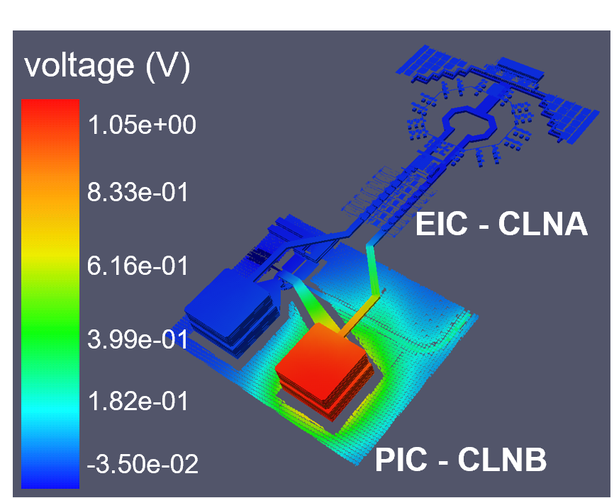
A 3DIC architecture allows the vertical interconnection between the PIC and the EIC contributing to the high-speed, low-latency, and low-loss communication.
After the user imports the connection file, PeakView® obtains the process information for two process technologies (e.g. CLNA and CLNB).
PeakView® performs an EM co-simulation of multiple process technologies in a combined environment.
IC-CoWoS Integration
2.5D architectures such as CoWoS also improves the horizontal interconnection of chips delivering high interconnection density compared to previous solutions.
PeakView®’s 3DIC tool reliably integrates this technology with traditional advanced node for IC-CoWoS co-simulations.
Accurate TSV EM modeling for backside power delivery networks and CoWoS is also supported.
In fact, PeakView®’s combination of EM and RLCK netlist provides a comprehensive model that accounts for the coating capacitance formed by the TSV coating layer.
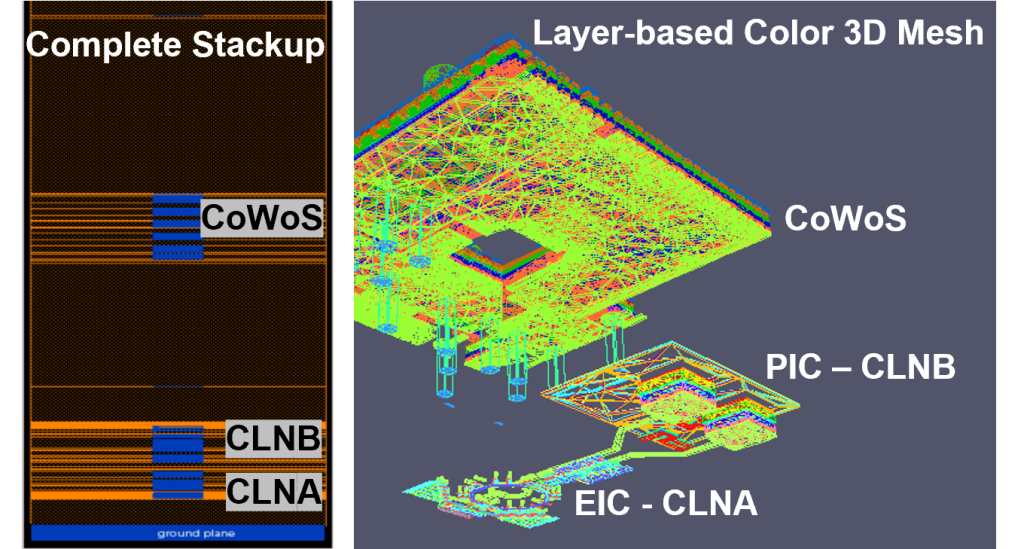
WoW-CoWoS Integration
PeakView®’s powerful 3DIC integration capabilities also extends to more complex systems, where both chips and CoWoS interposers are part of the modeling domain.
All PeakView®’s powerful EM analysis tools are also available for more complex integrations, which includes the 3D visualization of the mesh, voltage, current density, etc.
IC-Packaging Integration
IC-PKG co-simulation is crucial when evaluating coupling effects from the package, during the simulation of routing within the PKG layers, or for signal integrity analysis of the bump connections.
EM co-simulations of chips+packaging properly captures the induced current density produced by inductors on ground planes.
This current density impact the performance of passive leading to degradation.
IC-PKG-PCB Integration
PeakView®’s 3DIC/PKG™ has extended the design integration to unlimited architectures allowing the EM analysis of complete systems that may involve IC with PKG and even PCB routings.
IC, Packaging, and PCB EM problems are intertwined due to small size and high speed. Signal integrity may be compromised without EM co-sim.
References
LD22613_PeakView®’s EM Design Platform for Large-Scale 3DIC Systems in the New AI Era
LD20268_PeakView EM Design on TSMC CoWoS and IC-CoWoS EM Co-Simulation
LD19378_PeakView® Chip-Packaging-PCB EM Co-Sim
Lorentz Solution Inc. Electromagnetic Co-Simulation of Multi-Processes, Packaging and Systems. U.S. Patent Pending.
For Application Notes requests, please contact: support@lorentzsolution.com