
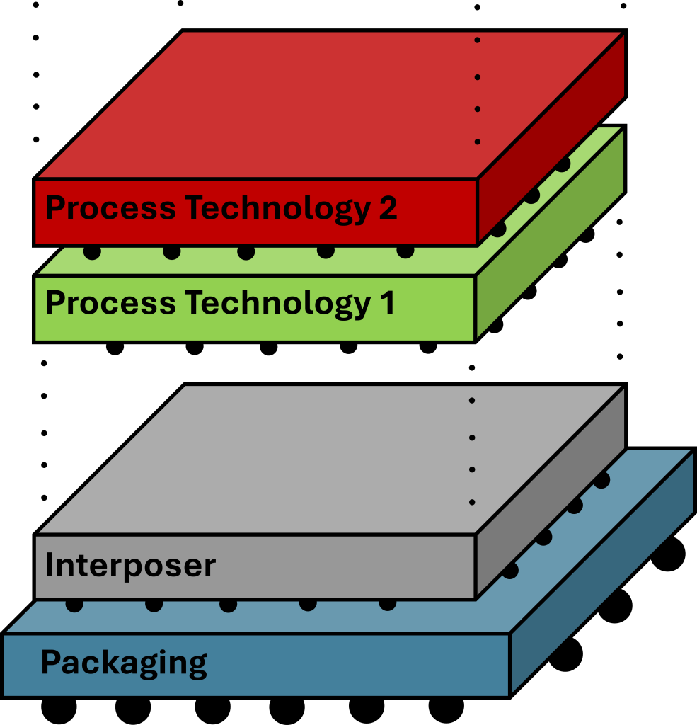
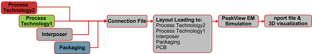
PeakView®’s design flow supports a multi-level IC/3DIC/Packaging EM co-simulation environment with unlimited layers and arbitrary combinations. This makes the 3DIC EM design and signoff a reality by seamlessly integrating multiple PDKs without requiring any PDK modification. This integration is done through a connection file, which provides the path for the different processes to be combined. This feature represents an efficient solution to address EM design challenges concerning chip-to-chip and chip-to-package interactions, supporting advanced integrations such as 3DIC (Wafer-On-Wafer), COUPE, CoWoS, conventional flip-chip packaging technologies, and even PCB designs.
3DIC/PKG™ Flow
- Lorentz Solution Inc. Electromagnetic Co-Simulation of Multi-Processes, Packaging and Systems. U.S. Patent Pending.
PeakView® is at the Forefront of the EM simulation of 3DIC and Packaging Designs with Key Technological Breakthroughs
-
- Process technology integration for the incremental addition of processes including advanced nodes
- Core EM solver technologies with 3D accuracy from DC to TeraHz frequencies for reliable modeling of thick layers and long vias (bumps and TSVs)
- High-performance and high-capacity EM solver capabilities for cases with millions of unknowns
- Flexible meshing techniques for full-chip EM simulations with sufficient accuracy in high-speed regions (coils, MIMCaps, incerconnects, etc) while maintaining coarse mesh on floating structures.
- Accurate EM modeling of IC, 3DIC, and Packaging building structures such as thick layers, bumps, and a comprehensive RF/mmWave model for Through Silicon Vias (TSV).
- Output models based on nport files and RLCK netlists with guaranteed passivity verification
3DIC/PKG™ High-Performance Features
3D EM Simulation Accuracy
-
- EM effects such as vertical skin depth, vertical inductance, vertical coupling, and conductive losses are only accurately captured with 3D accuracy, which becomes critical for stacked processes.
- 3D accuracy is critical for the accurate simulation of the vertical inductance for bumps, TSVs and long vias, which are building blocks of the latest process integration.

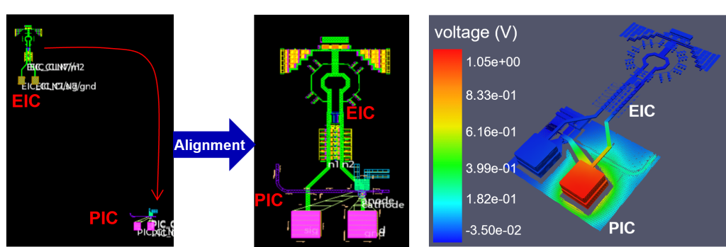
Combination and Alignment of Multi-Process Layouts with Combo Cell
-
- PeakView®’s Combo Cell is ideal for combining cell layouts, including layouts from different process technologies enabled by the 3DIC/PKG™ flow.
- Combo Cell also provides X- and Y-offsets for the user-friendly alignment of layouts with extremely high precision, which is necessary for complex 3DIC integration such as wafer-on-wafer.
Flexible Meshing Setup (FMS) for Multi-Process Meshing
-
- From the “Advanced…” options, the user can control the mesh size by assigning different mesh types to different layers.
- The structures in one process technology (PKG) may be bigger compared to the structures in another process technology; therefore, different mesh densities is required in different layers.
- The user can select onChipMMWave (fine mesh) globally and select RDL_Normal (coarser mesh) for the structures in the packaging process from PeakView®’s advanced options.

Supported Formats
- 3DIC/PKG™ Setup
- iRCX format technology file from TSMC
- ITF format technology file from foundries
- 3DIC/PKG™ Input
- GDSII format layout generated by Cadence® Allegro® or other tools.
- Standard Library PCircuit™ and user-defined PCircuit™
- ODB++ Import
- 3DIC/PKG™ Output
- n-port, Physics-Based EM models.
- Cadence® library views, i.e. DRC clean layout, schematic symbols, etc.
- Multi-corner and temperature-dependent models.
- ODB++ Export
- Platform
- Linux 64 bit, i.e. Redhat and SUSE
- LSF, NC-based computing farm