
Overview
 PeakView’s LEM™ solution uses multisheet current (MSC) setting as an effective volume meshing technique to model vertical current distribution and vertical inductance phenomenon, hence 3D full-wave effects can be modeled; a definite step up from the subpar Planar-3D approach still seen by our competitor.
A single click from within the Cadence Virtuoso® or Synopsys Custom Compiler™ layout views allows passive and interconnect structures to be extracted for 3D electromagnetic analysis. PeakView’s high-capacity EM engine supports complex multi-port structures and swiftly creates accurate EM models and corresponding views in the design library.
LEM™ enables designers to incrementally adjust the parameters of devices during design process and supports composite layouts with passives, interconnect, DFM structures (e.g. metal-fill) and wafer scale package elements to be accurately EM analyzed with LEM.
Benefits
- Accuracy, Performance and Capacity
PeakView’s patented EM solver combines high accuracy, computational performance and capacity needed to analyze complex layouts with devices, interconnect and Packaging and 3D-IC interfaces. It matches silicon accuracy and supports frequencies from DC – mmWave –Terahertz range.
- Support for Advanced Process Nodes and Technology
LEM support for advanced process nodes from 65nm to 3nm PDKs with the most up-to-date design rules and utilities (i.e. metal-fill). PeakView’s iRCX and ITF Parsers simplify importing PDK layer process information into the tool. All process nodes with any metal stack-up are supported in LEM™.
- Design Flow Integration
LEMTM is seamlessly integrated into the Virtuoso® and Custom Compiler™ layout editors with a bi-directional, lossless data exchange interface. Designers are able utilize the tool in their familiar IC design environment.
- Automates Layout Processing
PeakView™ automatically processes compound designs and generates corresponding layouts for EM simulation. The layouts are algorithmically verified and modeled; users are not required to make any modification (e.g. simplifying via, metal fill etc.) to their designs. With automated internal layout processing, PeakView™ LEM.
LEM™ Features
Advanced EM Modeling Features

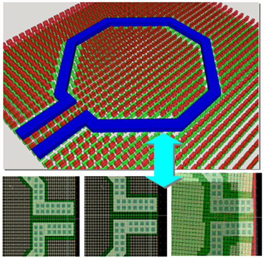
1. Support for DFM Requirements such as Metal Fills and Slotting
PeakView is a Full-Wave EM Solver with 3D Accuracy that overcame these difficulties through rigorous meshing techniques and EM equations. PeakView uses volume meshing to capture the effect on side walls (side-wall capacitance) and calculates the current density in multiple sheets forms on a conductor to include the skin effect at high frequency. As a result, vertical inductance may be considered.

2. Support for DFM Requirements such as Metal Fills and Slotting
LEM™ addresses sub-40nm challenges in advanced processes with the PeakView™ chemical-mechanical polishing (CMP) option. This feature allows LEM™ to accurately simulate and model complex metal slotting, striping, and via arrays, aiding time-efficient automated design. It provides comprehensive modeling methods for dummy metal fill with passive devices over all frequency ranges.
PeakView™ LEM for Layouts with Devices and Interconnect
PeakView LEM™, in conjunction with CMP™, provides full support for advanced process node DFM requirements during EM synthesis and Layout EM extraction. Designers are able to define their own metal fill and slotting requirements in the PCircuit parameters. During EM synthesis these rules are considered and PeakView delivers a DRC clean layout with the industry’s most accurate EM and circuit simulation models.
3. Physics-Based Modeling
In addition to purely numerical n-port S-parameter models, LEM™ also provides the option to generate compact RLCK models called Physics-Based Models (PBM) that guarantee passivity and physical realizability. PBM generates EM models as Spectre or HSPICE™ equivalent sub-circuits for use in transient simulations. PBM models are guaranteed to be convergent and passive over a user selectable frequency range. PBM preserves the DC inductance and resistance, and does not shift the circuit’s operating point. In addition, PeakView PBM automatically ensures that the model correctly accounts for white noise content.
Interconnect with irregular or non-uniform structures can also be modeled with 2nd generation Physics-based Models (PBM2). PBM2-based LEM is able to convert S-parameter models of arbitrary geometries with high port counts into compact equivalent circuit models that can be used in time-domain circuit simulations. When combining LEM with HFD for EM integrity analysis on coupling groups makes it easier to detect and repair EM integrity issues at circuit level. This enables designers to easily perform transient simulations of their designs with EM-level accuracy..
4. Hierarchical PBM (HPBM)
PeakView™ HPBM has been developed to address the modeling of complicated structures by bringing in an innovative hierarchical view to the modeling process. In the HPBM flow, user can specify different PBM methods for each sub-component. PeakView will then produce a single PBM model of the entire design by combining the sub-component models and adding coupling effects between them.

Tool Integration
1. Process Corner and Temperature Coefficient Modeling
PeakView™ generates S-parameter and lumped models that account for process corner and temperature sweeps. Foundries provide several types of technology files in terms of Rbest, Rworst etc., that reflects process variations. Temperature coefficients of materials are also obtained from technology files. PeakView™ generated corner based model files accounting for process corners and temperature coefficient analysis and can be synced to the design library. The models can be utilized within popular simulation environments such as ADE-XL.
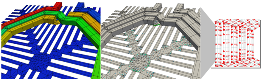
2. Visualization
PeakView LEM’s visualization system expedites debugging of device design by showing the EM mesh, voltages, currents and charge distribution. Inaccuracies in the structures are apparent early and can be fixed preemptively in the design phase. The built-in visualization window provides for better understanding of skin effects and capacitive coupling, image currents at various frequencies. The chart window plots pre-defined and user-defined quantities of interest from EM simulation results.
Voltage and charge visualization LEM simulations are shown in the following figure..
High-Performance Features
1. Flexible Meshing for Customized Accuracy Types
In addition to pre-configured EM simulation types, PeakView™ has implemented Pre-Customized Accuracy Types to enhance the flexibility of accuracy settings and to configure layout processing and EM simulation options. By composing a configuration file, users are able to easily tune the tool such that the entire EM simulation process is optimized for special test cases. This is particularly useful for scenarios where concurrent simulation for structures of varying scales is required. “It’s as easy as wit
2. Multi-core Processing and Distributed Computing
In order to maximize utilization of computing resources, LEM™ takes advantage of PeakView’s multi-core processing capability. Design jobs can be run on compute farms consisting of multi-core machines, as well as on standalone platforms with multi-processor hardware to achieve maximum efficiency of computing resources. PeakView provides different distributed computing modes to concurrently accelerate the EM modeling. Users are able to specify different frequency points to be simulated on different machines in a computer farm.
3. Revolutionary EM Solver Technology
Direct Solver Engine:
• Quick EM technology to drastically boost simulation performance without the loss of accuracy.
• Added GPU and CPU/GPU performance enhancements capability.
Iterative High Capacity Solver (HCS):
• 5 to 30x memory reduction while maintaining within 1% accuracy of 3D full-wave direct solver accuracy.
• Ideal for large scale EM simulations, such as metal fill, full chip, IC-Pkg-PCB and 3D-IC Co-simulation.
LEM™ Flow
The PeakView LEMTM flow accommodates three different modeling approaches frequently used by designers. For Layout EM analysis users can: 1. launch LEM™ from within their Virtuoso® environment and export their layouts to PeakView™, 2. Import a GDSII format layout file into PeakView™ or, 3. Synthesize a layout in PeakView™ using PCircuits.
Design layouts that contain compound structures of varying scales (on-chip devices, large RDL lines, PCBs, planar package elements) and contours (polygons of any angles, circular via holes, curved paths) are accurately processed by LEM™.
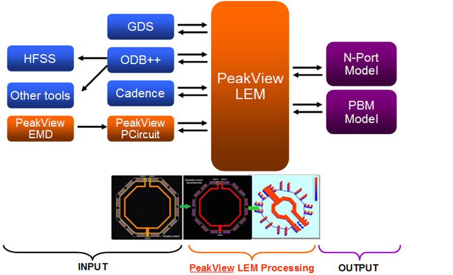
LEM™ Flow
LEM™ generates a corresponding layout in the PeakView™ GUI. PeakView’s high precision EM engine is then used to electromagnetically analyze the layout and create relevant views corresponding to the EM models. Generated views are then synced to the Virtuoso® Library to be used for SPICE simulation.
Applications
LEM™ is useful for a wide variety of applications in semiconductor design. LEM, based on PeakView™ high precision, 3D EM solver, performs accurate signal integrity analysis on complex layouts consisting of a broad class of elements. LEM™ efficiently characterizes broadband (e.g. clock-lines), as well as narrowband (e.g. LNAs) applications, from DC to the sub-THz spectrum.

LEM™ Applications
Applications include, but are not limited to:
- Passive Devices
Inductors, MOM capacitors, MIM capacitors, baluns, transformers and commonly used device topologies and associated metal fill, guard-rings, patterned ground shields, etc.
- Interconnect
Microstrip lines, co-planar waveguide (CPW) lines, T and X junctions and other planar transmission media or signal routing.
- DFM Structures
Metal fill, wide-metal slotting, striping in advanced process nodes (20nm and beyond)
- Board-level Analysis
PCB coupling effects (e.g. sensor placement for board-level analysis, feedback impedance return path via ground planes)
- Wafer-Scale Package Elements
Coupling between planar wafer-scale package elements and on-chip passives
Supported Formats
- LEM Setup
- iRCX format technology file from TSMC
- ITF format technology file from foundries
- LEM Input
- Virtuoso® or Custom Compiler™ layout with pins
- GDSII Layout
- ODB++ Import
- PCircuit
- LEM Output
- n-port, Physics-Based EM models.
- Model views added to Cadence® Library.
- Platform
- Linux 64 bit, i.e. Redhat and SUSE
- LSF, NC -based computing farm