
Overview
We have developed a user-friendly, novel utility Chip/Packaging EM Co- Simulation™ equipped for IC, package, and board-level electromagnetic coupling analysis. The utility expands the application of PeakView LEM™ to include package and PCB signal integrity analysis in a simplified user interface.
Peakview IC/PKG co-sim including:
-
- Vertical inductance and current with full-wave EM simulation;
- Incremental PKG profile combined with PDK baseline provides OA/GDS/ODB++ support;
- Layer meshing and powerful EM analysis features (visualization etc.)
Further, PeakView HFD extends 3DIC RC extraction flow to include inductance and full-wave models for critical nets. These capabilities allow 3DIC having the best RLCK and full-wave extraction flow for today’s RF, mmWave and high-speed analog designs.
 Benefits
PCB Impedance Analysis
At high frequencies, as noise currents and electromagnetic coupling to PCB traces increase, a full-system, EM analysis is necessary to examine the frequency-dependent impedances in the supply paths and to determine the placement of sensitive circuitry on the board. IC/PKG EM Co-Sim™, with an accurate PCB impedance analysis, assists designers to:
- Minimize unintended radiation caused by loop currents through ground return paths.
- Minimize noise in high impedance power distribution networks, where noise-level is proportional to the currents.
- Ensure stability of the AC reference, since impedances on the AC ground is impacted by PCB design.
- Reduce ground bounces due to high- speed IC switching events that introduce unpredictability to the circuit characteristics.
Package and On-chip Layout Co-existence & Processing Capability
Simultaneous simulation of co-existing package structures and on-chip devices warrant sophisticated CAD geometry processing capabilities. Devices (e.g. on-chip passives) and package elements (e.g. via pillars, solder bumps) vary markedly in size. IC/PKG EM Co-Sim™ provides a full-system analysis of all components of varying scales with accurate meshing.
Meshing Circular Paths and Via Holes
Unlike devices with straight-line or polygonal contours, packaging structures often contain circular geometry or arbitrary curly shapes. The meshing of circular paths and holes are given specialized consideration to obtain an optimal balance in accuracy and computing cost.
High-speed Switching
Spurious electromagnetic emissions can arise from high-speed CMOS switching circuits or current impulses from clock signals through gates. IC/PKG EM Co-Sim is able to examine these events in transient circuit simulations with numerically convergent, passive PBM models.
IC/PKG EM Co-Simulation™ Features
Advanced EM Modeling Features
1. Simple Incremental Profile Approach
The metal stack information of IC and packaging layers are different. PeakView™ has incorporated an ‘Incremental Profile’ approach. Instead of modifying the base profile, the incremental profile is just an add-on to that which is based on specific packaging needs. This feature is particularly important as nowadays, all of the advanced node profiles are encrypted. In this approach, the original IC profile file remains unchanged.
2. Large-Capacity Solution Space
The PeakView™ IC/PKG EM Co-Sim utility is built as an extension to our current LEM (Layout EM) feature. The board-package-level solution has the computational power to handle electromagnetic problems that would otherwise require memory in the order of (Terabytes) TBs.
 SPICE Simulation-ready PeakView™ Models for PCB Traces
PeakView™ uses GDS data transfers for full-board simulation with multi-layer PCBs. Applications include placement of sensitive magnetic sensors in optimum PCB locations that ensure minimal board impact.
In our present capability, the Peakview™ 3D solver obtains board-level input from PCB design tools (i.e. Cadence® Allegro®) and generates a SPICE simulation-ready model in a very short time.
3. Simplified Layout Processing
IC/PKG EM Co-Sim™ processes PCB geometry generated by Cadence® Allegro® in .gds file format and generates a corresponding layout for full-wave simulation; users are not required to make any modification or simplification to their designs. PeakView™ uses efficient strategies to handle PCB and packaging layouts without compromising simulation accuracy.

4. EM Solver Capability for On-Chip and Packaging Structure
A combined on-chip and packaging structure require separate EM simulation settings for a substantial EM modeling: dense mesh for on-chip structure and coarse mesh for packaging structure. PeakView IC/PKG EM Co-Sim feature is compliant to initiate required settings.
5. Meshing
Advanced meshing algorithms are used to preserve details of circular or atypical contours in boards and planar elements in the design. The meshing mechanism provides scale-specific processing of on-chip and package-level structures. Vias, polygons, curved surfaces, and intersections are optimally meshed and quickly solved by the simulation engine.
Tool Integration
1. Allegro Interface
PeakView™ is able to directly import layouts in .gds format. If Virtuoso® Layout Editor is used to invoke Allegro®, then PeakView™ is also able to utilize this interface as a data exchange channel. In the latter case, Peakview LEM™ can be launched from the Virtuoso® IC environment to analyze the layout created in Allegro®. All pins will be loaded automatically for the packaging structure as ports.
2. ODB++ Interface
ODB++ provides an intelligent, single data-structure for PCB design, including features, vias, pins, etc. It has been widely used by PCB design and manufacturing organizations.
PeakView™ is able to import ODB++ format which supports by most of the 3rd party PCB/package design tools. Users can easily import geometries from their desired PCB/packaged design tools to PeakView including automatic loading of all the pins for EM simulation. PeakView™ is also able to export the ODB++ format. It can then be imported to a true 3D EM simulator, such as Ansys, AWR, CST, etc, for system-level simulation.
High-Performance Features
1. Customized Accuracy Types
Customized Simulation Type is a feature implemented to enhance the flexibility of PeakView™ and to allow users to configure layout processing and simulation options in addition to pre-configured EM simulation types. By composing a configuration file, users are able to perform concurrent simulation for structures of varying scales in the chip-package co-design.
2. EM Key Challenges
For IC/PKG EM Co-Simulation, the vertical current through thick conductors can be being simulated.
- Vertical inductance (including mutual vertical inductance) is difficult to capture.
- Vertical inductance of vias
- Vertical inductance of thick metal
- All the coupling among vertical currents.
Using rigorous vertical meshing and EM equations, PeakView effectively captures vertical inductance, vertical resistance as well as sidewall capacitance of vias and thick metals.

Field Visualization of Vertical Inductance of Via-Metal Stack
3. Multi-Sheet Current (MSC)
To circumvent huge computing overhead for volume meshing in order to achieve 3D accuracy, PeakView provides MSC as an effective volume meshing method to capture vertical current distribution and vertical current and inductance effects. As result, to achieve convergence for 3D accuracy of a path structured mesh has been accelerated dramatically. For a simple structure with path mesh, the setting of MSC=1 can be sufficient, while combined structures of polygon and path mesh can use higher MSC setting to achieve equivalent accuracy.
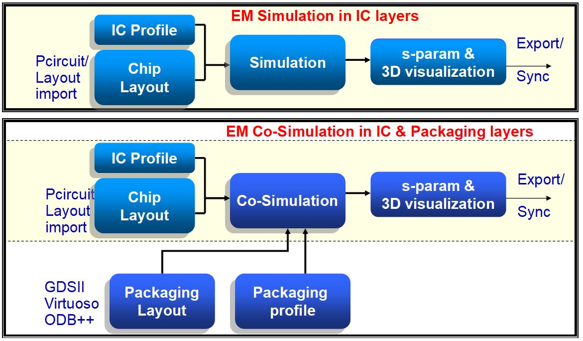
IC/PKG EM Co-Simulation™ Flow
The PeakView IC/PKG EM Co-SimTM flow enables users to import layout structure into PeakView using Virtuoso, GDS, or ODB++ methods. Design contains structures of varying scales (on-chip devices, large RDL lines, PCBs, planar package elements) and contours (polygons of any angles, circular via holes, curved paths) are accurately processed by LEM™.
The incremental profile that contains the packaging layer information leaves the IC baseline profile unchanged. PeakView’s EM engine then simulate the layout and create relevant EM models and corresponding views that can be synced to the Virtuoso® Library to be used for SPICE simulation.
Supported Formats
- IC/PKG EM Co-Sim Setup
- iRCX format technology file from TSMC
- ITF format technology file from foundries
- IC/PKG EM Co-Sim Input
- GDSII format layout generated by Cadence® Allegro® or other tools.
- ODB++ Import
- IC/PKG EM Co-Sim Output
- n-port, Physics-Based EM models.
- Model views added to Cadence® Library.
- ODB++ Export
- Platform
- Linux 64 bit, i.e. Redhat and SUSE
- LSF-based computing farm